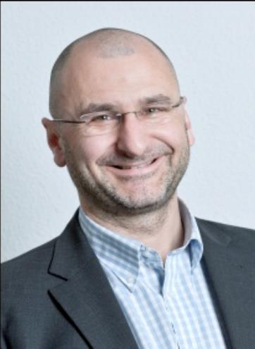
报告题目:Smart Device Architectures For Organic & Perovskite Solar Cells
报告人:Prof. Christoph J. Brabec
Institute of Materials for Electronics and Energy Technology (I-MEET)
Friedrich-Alexander-University Erlangen-Nuremberg, Germany
地点:907#楼1101室
时间:2015年07月16日(星期四) 上午9:00

报告人简介
Academic & industrial development
1996: Sabbatical at the Institute for Polymers & Organic Solids at the University of California, Santa Barbara (Prof. Alan J. HEEGER, Nobel laureate 2000 for Chemistry)
1998 - 2001: Principal Investigator (PI) at the CD Laboratory for Plastic Solar Cells, Linz, AT
2001 - 2004 Principal research scientist & project leader at Siemens Corporate Technology, Department Microsystems and Materials, Erlangen, Germany
2004 - 2009: Various positions at Konarka Technologies after a successful outsourcing of the organic photovoltaics activities from Siemens
08/2004: Appointment to Director of OPV at Konarka Technologies, Lowell, USA
2005: Appointment to the CEO for Konarka Austria and Konarka Nuremberg
04/2006: Appointment to the CTO and Vice President at Konarka Technologies, Lowell, USA
2009 - aktuell: W3 Professor at FAU University Erlangen-Nuremberg (Institute Materials for Electronics and Energy Technology – I.MEET)
2009 Appointment to the scientific director of the ZAE Bayern, Erlangen
2009 Appointment as Executive Board Member of the ZAE Bayern
2010 Appointment as Board Member of the Energy Campus Nürnberg (EnCN) eV
2013 Appointed as Speaker of the International Center for Nanostructured Films (IZNF) at FAU Erlangen-Nürnerbg
2013 Appointed as Head of Board of ZAE Bayern eV
Publications: > 300 publications in ISI rated journals, h factor > 70, > 90 patents
Scientific Research Interest:
●Research and development on solution processed semiconductors, with a strong focus on the photophysics and transport properties of disordered semiconductors.
●Investigation of microstructure & morphology formation in thin films
●Development of printing and coating technologies for electronics and semiconductors
●3rd generation solar cell technologies.
●Development and application of non-destructive imaging methods for optoelectronic devices
●Renewable energy systems and components for energy generation and storage
Awards / Functions:
2005 “Inventor of the year” with the highest number of patents in the field of organic PV
2007 Rated among the top ten cited researchers in the field of organic electronics / solar cells
2011 Ranked as #12 among the top 100 material scientists for the last decade (by ISI) ngoing Serving in boards or as editor for multiple journals
